
2025 IEEE ECTC Press Kit
Welcome to the Editor Press Center. The following press materials may be downloaded from this site for news coverage of the 2025 IEEE ECTC.
Contacts
Gary Dagastine
co-Media Relations Director
+1 518 785 2724
[email protected]
Chris Burke
co-Media Relations Director
[email protected]
2025 IEEE ECTC Press Releases:
Welcome to the Editor Press Center. Check back periodically for photo and caption updates.
- 2025 ECTC Technical Tipsheet
- Student Engagement and Involvement is a Major Focus of the Upcoming 75th Annual IEEE Electronic Components and Technology Conference
- 2025 IEEE Electronic Components and Technology Conference Highlights Microelectronics Packaging and Component Breakthroughs
- 2025 IEEE Electronic Components and Technology Conference Announces Student Competition; Proposals Must be Submitted by November 30, 2024
- ECTC 2025 Call for Papers
News Coverage:
- Semiecosystem (5/21)
- 3D InCites (5/1)
- Silicon Semiconductor (U.K., 4/28)
- EMS Now (4/25)
- PCB Directory (4/25)
- TimesTech (India, 4/25)
- Semiconductor Digest (4/24)
- Chip Scale Review (March/April 2025 issue)
- ElectronicsBuzz (India, 4/25/25)
- Mat Dirjish Online (4/15)
- Semiconductor Engineering (4/2)
- Semiconductor Engineering (4/25)
- Elektroniknet (Germany, 1/21)
2025 IEEE ECTC Photos with captions:
Selected images from the papers will be presented in two formats:
– Word file with images associated with a highlighted paper and the caption
– JPEG OR PNG file with individual high-resolution images
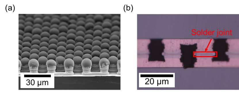
Paper 1.2, Face-Down Bonding and Heterogeneous Chiplet Integration by Using Bumpless Chip-on-Wafer (COW) with Waffle Wafer Technology, Y. Satake et al, Murata - Institute of Science Tokyo - Panasonic Connect Co. Ltd
Paper 2.6, All-SMF Arrays for Co-Packaged Optics – Optimizing Cost, Complexity and Performance, N. Mehta et al, NVIDIA
Paper 4.1, Package Warpage Reduction for Large CoWoS-R Packages, Yu-Hsiang et al, TSMC
Paper 5.6, RF Si Interposer Platform for Chiplet-based Heterogenous Systems, X, Sun et al, IMECn
Paper 9.4, Self-formed Barrier using Cu-Mn Alloy Seed applied to a 400nm Pitch Wafer-to-Wafer Hybrid Bonding Technology, S. Van Huylenbroeck et al, IMEC
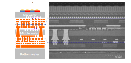
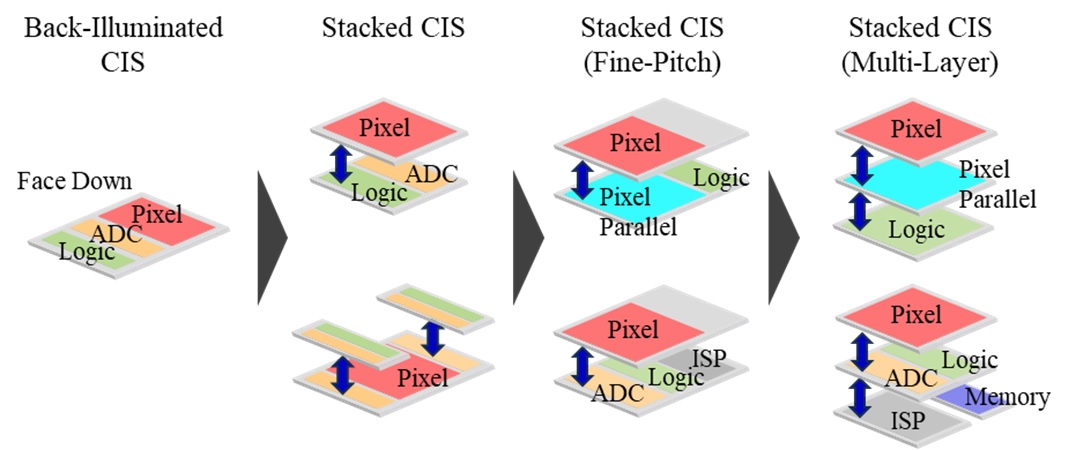
Paper 14.4, Development of A Novel WoWoW Process for 1 and 1.3-inch 50 Megapixel Three-Wafer-Stacked CMOS Image Sensor with DNN Circuits, K. Shimizu et al, Sony
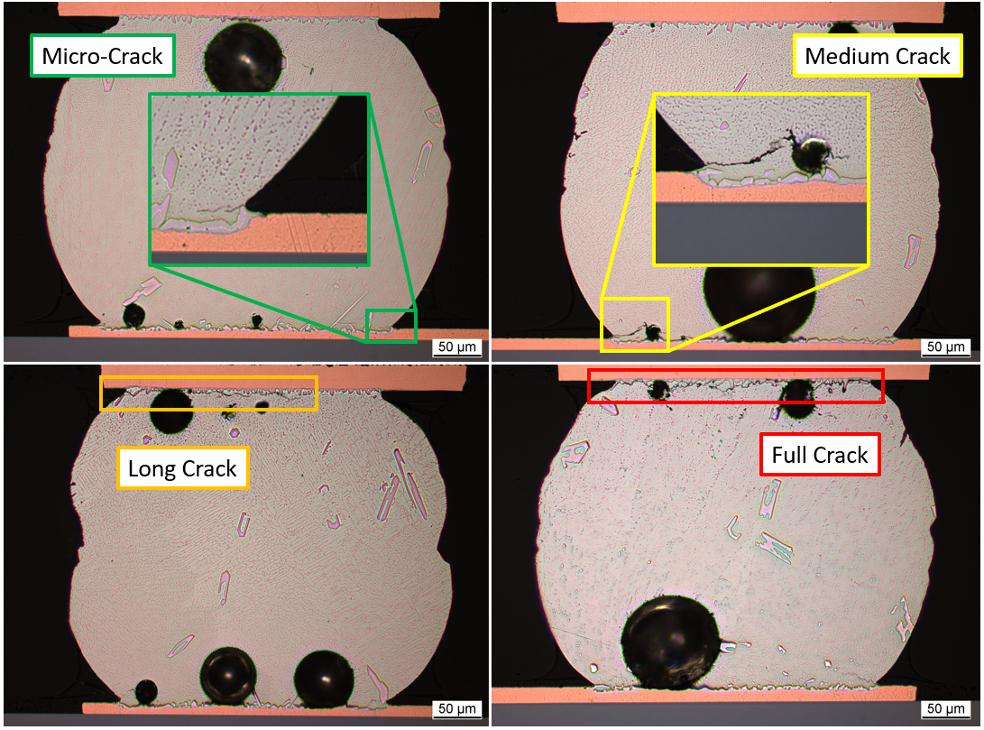
Paper 18.7, Isothermal Shock Testing on Flip-Chip Interconnects, M. H�usler et al, TU Dresden
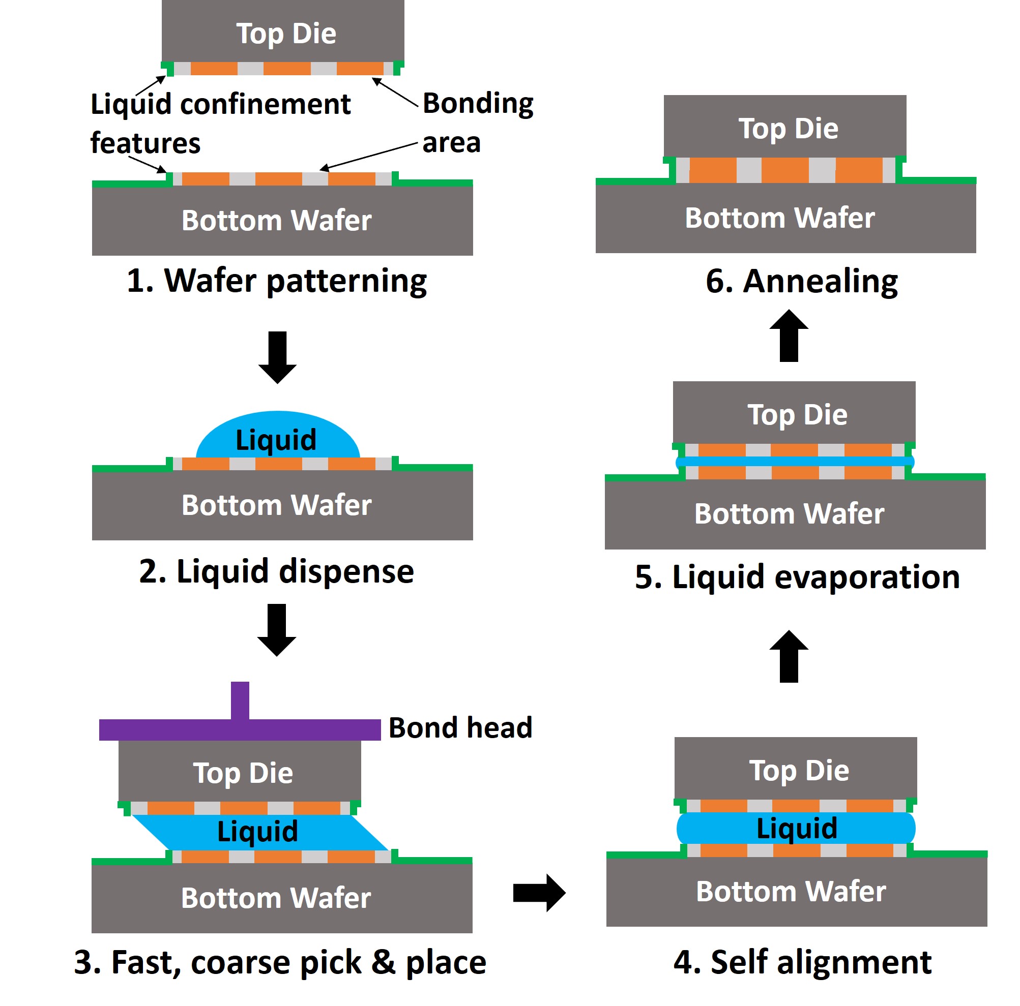
Paper 22.1, Hybrid Bonding with Fluidic Self Alignment - Process Optimization and Electrical Test Vehicle Fabrication, F. Eid et al, Intel
Paper 24.5, Predictive Modelling of Thin Films Properties Using An Experimental and Simulation-Based Approach, D.K. Lim et al, Nat’l Univ. of Singapore and Micron Technology
Paper 28.5, The Influence of Full IMC Structure on Micro-Bump Electromigration Performance, Chung-Yu Chiu et al, TSMC
Paper 29.5, Design and Fabrication of Bendable Double-layer RDL Metallization Based on FOWLP for In-Mold Flexible Hybrid Electronics (iFHE), C. Liu et al, Tohoku Univ
Paper 31.5, Localized Formation of Laser Non-Conductive Film (NCF) on 10 µm Diameter Bumps, Applied to 20 µm Pitch Chiplet Chip-on-Wafer (CoW) Bonding, J. Shin et al, ETRI - Hanbat National Uni
Paper 32.3, Ultra-Fast Cu Polymer Hybrid Bonding with Electroless Passivation Layer for Cost-Effective High IO Interconnection Stacking, Yu-Lun Liu et al, National Yang Ming Chiao Tung Univ. and Tokyo Ohka Kogyo Co. LTD
IP session 37, Fast And Accurate Machine Learning Prediction of Back-End-Of-Line Thermal Resistances in Backside Power Delivery and Chiplet Architectures, P. Chowdhury et al, IBM
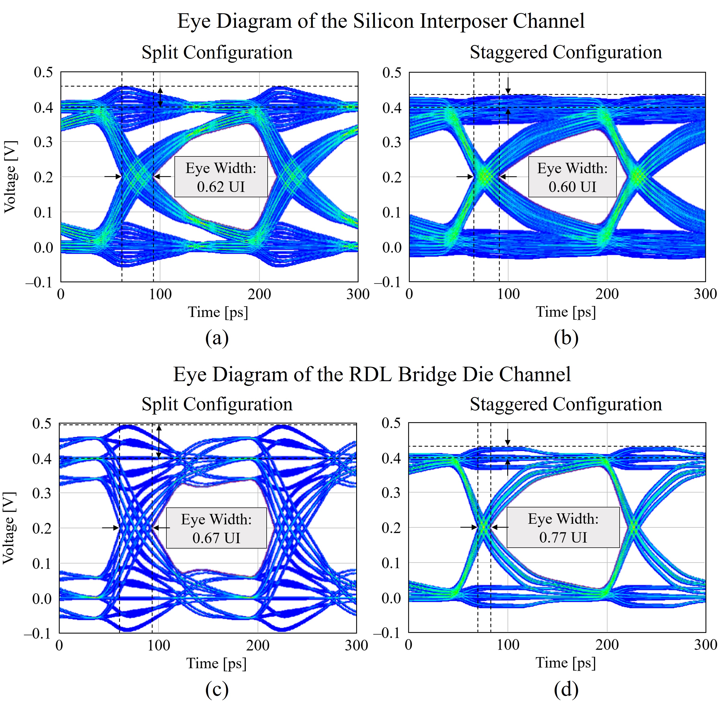
IP session 38, Signal and Power Integrity Optimization Using Novel Bridge Die and Copper Post Interconnect Design in 2.xD Packaging for Wide IO Applications, Y. Na et al, HANA Micron Inc. - Myongji University - Swevenz Inc
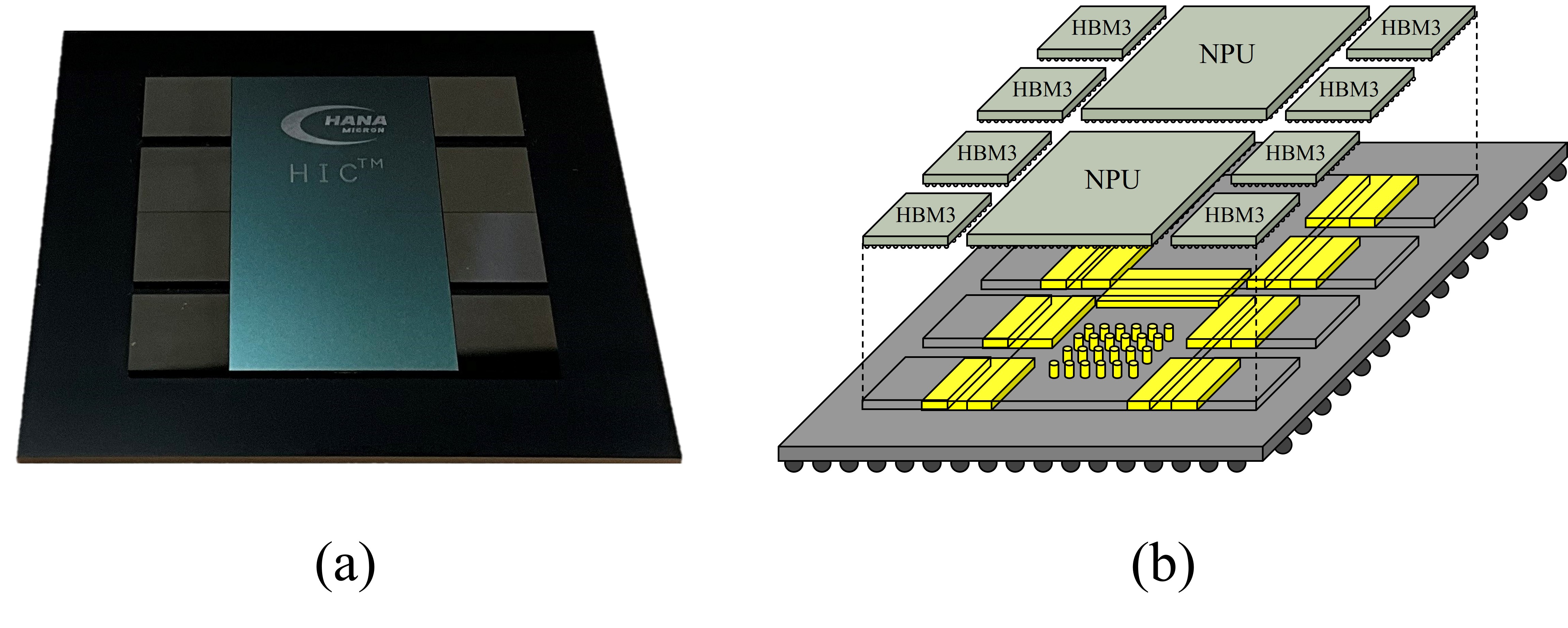
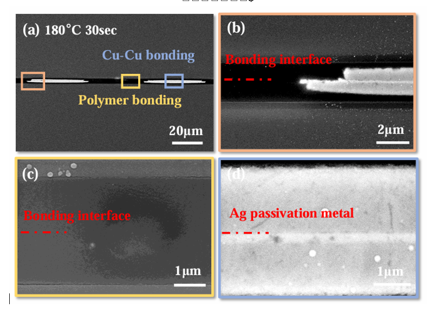
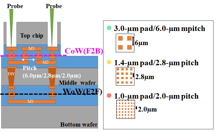
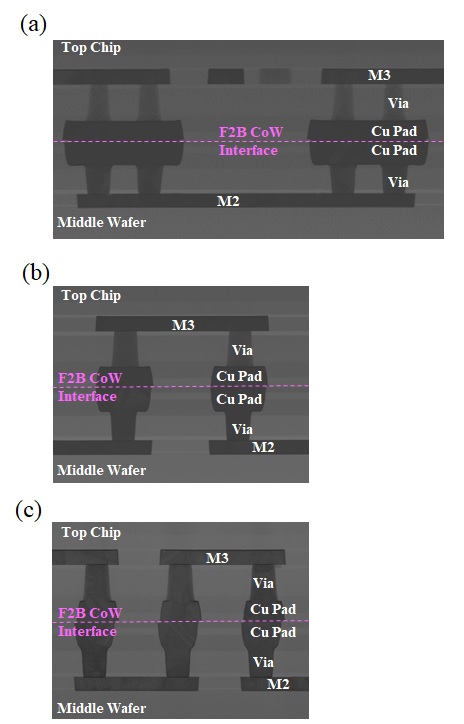
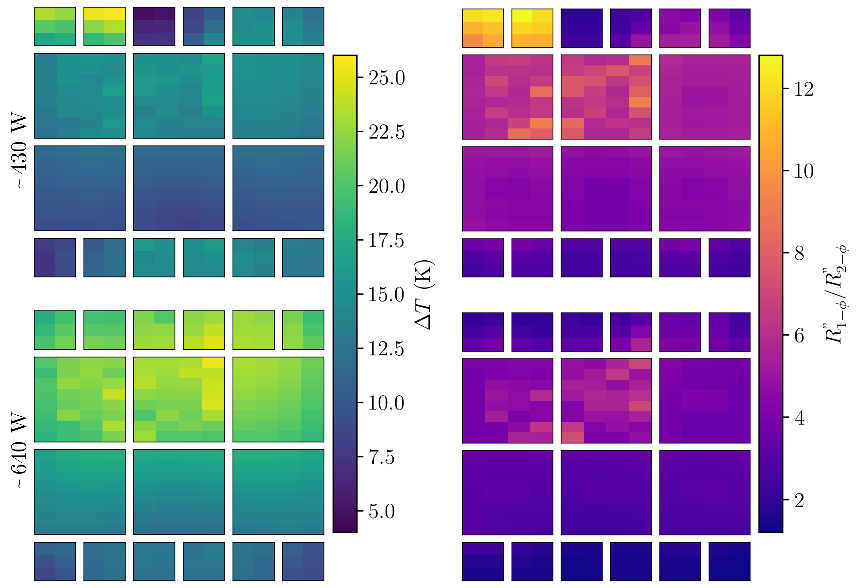
IP session 39, Advanced Face-To-Back CoW 2.0-µm pitch Cu–Cu Hybrid Bonding Process for Three Layer-Stacked 3D Heterogeneous Integration, A. Urata et al, Sony
- IP Session 39 Figures 1, 5 and 13 with caption
- IP Session 39 Figure 1
- IP Session 39 Figure 5
- IP Session 39 Figure 13
IP session 40, Experimental Demonstration of High-Power Thermal Test Vehicle using Two-Phase Cooling for AI Datacenters, 5G RAN, and Edge Compute Nodes, Yang Liu et al, Nokia Bell Labs
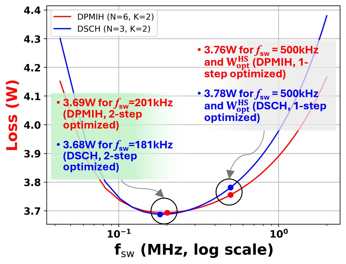
IP session 41, Hybrid Voltage Regulators for High Performance Computing - Analytical Models and Design Methodology, S. Abdelzaher et al, University of Illinois
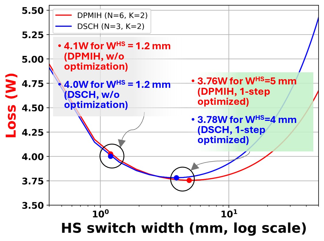
Previous Conference Press Kit Information:
General registration/attendance questions can be answered by Lisa Renzi, at [email protected]
About IEEE & EPS
IEEE is the world’s largest technical professional organization dedicated to advancing technology for the benefit of humanity. Through its highly cited publications, conferences, technology standards, and professional and educational activities, IEEE is the trusted voice on a wide variety of areas ranging from aerospace systems, computers and telecommunications, to biomedical engineering, electric power, and consumer electronics.
The IEEE’s Electronics Packaging Society (EPS) sponsors the ECTC conference. EPS is the leading international forum for scientists and engineers engaged in research, design and development of revolutionary advances in microsystems packaging and manufacturing. Its areas of interest encompass all aspects of packaging and integration of electrical, electronic, optoelectronic, biological, micromechanical and sensing components.